
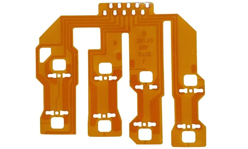
Check whether one layer can complete the routing
Map every signal and return path before selecting this construction. A one-layer outline that requires awkward external jumpers may complicate assembly. Compare that compromise with two-layer fabrication, especially where connector pin order forces conductor crossings. Treat shield and ground requirements as electrical functions, not optional labels.
One-layer construction decisions
| Feature | Define | Reason |
|---|---|---|
| Routing | Net order and conductor crossings | Determine whether one plane is sufficient |
| Protection | Coverlay and contact openings | Separate insulated and exposed copper |
| Termination | Contact face and reinforced thickness | Match the mating interface |
Describe the full local stack
The copper layer count is not the finished thickness. Base film, adhesive where used, coverlay, surface finish and reinforcement all affect relevant regions. Use a single-layer stackup drawing to identify what exists at the moving ribbon, exposed contact and soldered end.
State the required terminal contact side and where openings permit access. If both sides need accessible conductors, ask whether a specifically defined access construction is appropriate; do not assume that single-sided means any desired pad is available from either face.
Plan acceptance at the interfaces
List the dimensions that control fit: outline near an enclosure slot, terminal width, contact length and reinforced thickness. Identify installation bends separately from repeated movement. For a soldered end, include support and strain relief in the assembly discussion. Inspection should check the features that make the circuit usable, together with the agreed electrical test.
Before you release the design
- Review net order against the connector pinout.
- Dimension exposed copper and protective-film openings separately.
- Identify supported solder areas and moving sections.
- Send flat outline, installed view and revision-controlled net data.
Watch points
- A low copper-layer count does not remove connector, motion or assembly qualification work.
Practical questions
Is single-sided flex always the lowest-cost option?
Not necessarily. A larger outline, extra assembly connections or difficult nesting can outweigh simpler fabrication. Compare complete installed solutions using the same required functions.
Can a single-layer circuit be used for repeated motion?
Layer count alone cannot answer that. Specify the local stack, bend path, mounting, cycle requirement and environment, then agree a representative test.
Technical references
References support the material or design context. Check the exact grade, part number, document revision and project conditions before release.Updated 27 September 2026 · Technical content policy · Engineering guidance supports project review; the agreed drawing defines the build.